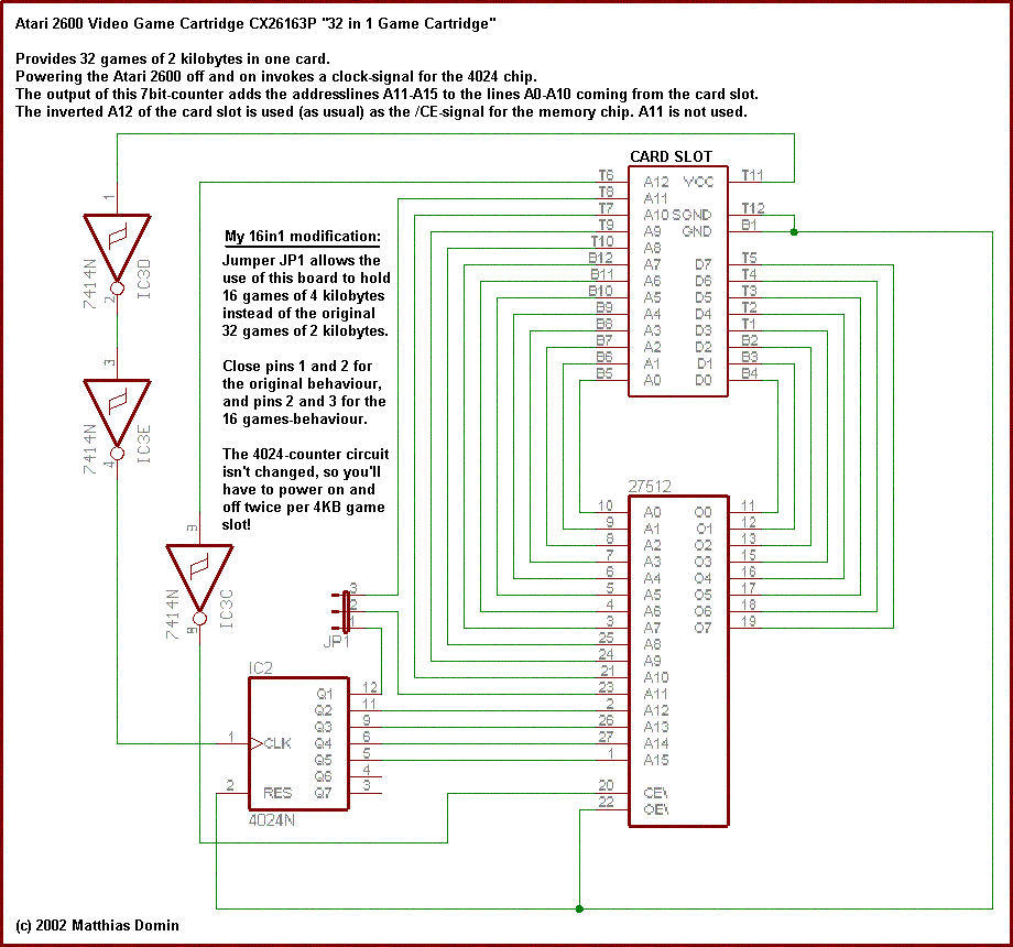
Here is a schematic of this modification:
You'll need:
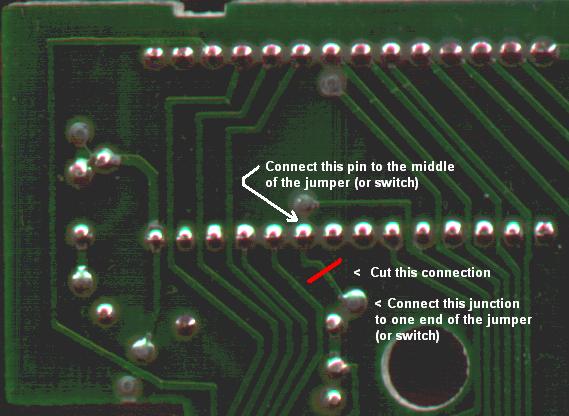
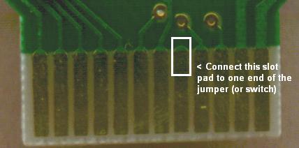
Step 2:
Drill 3 holes for the jumper into the PCB near the 6 resistors for
the datalines d0-d5 and insert the jumper into these holes.
Step 3:
a) Connect pin 23 of the PROM socket with the center pin of the jumper
(or switch).
b) Connect the PCB-junction of the A14 ddressline to one end of the
jumper.
c) Connect card slot pad Top8 to the other end of the jumper.
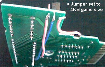
This pictures will help you going through steps 1-3:
Here is a picture of how it looks if you use a switch inserted in the
center hole of the PCB to choose between 2KB and 4KB access:
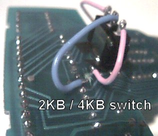
The blue wire connects the switch to pin 23 (A14) of the PROM socket.
The two pink wires are the two sources for A14.
Using a jumper field instead of a switch it can look like this: