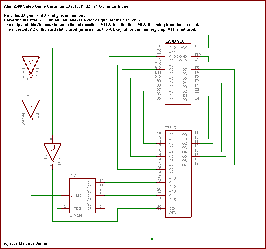
Here is an abstract schematic of this PCB:
Take a look at this modification if you
would like to play 16 games of 4KB each instead of 32 games of 2 KB with
this PCB.
Here are some pictures of the PCB of the 32in1 card:
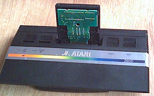
As you can see, when playing you are normally facing the soldering
side of the PCB.
The top side of the PCB (Move mouse over the several parts to get infos
about them):
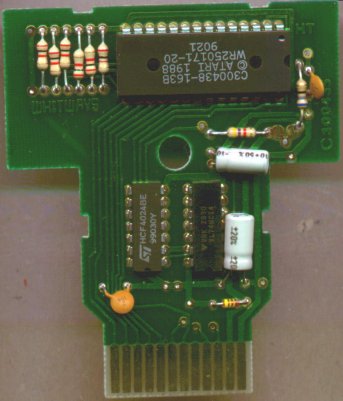
Without the PROM:
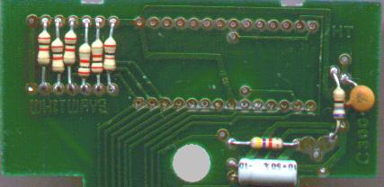
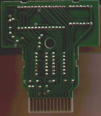
Bottom (soldering ) side of the card (Move mouse over the several parts
to get infos about them):
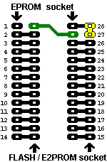
Because it is more convenient to use an E2PROM or a FLASH-ROM instead
of EPROMs (which have to be erased using UV-light), but FLASH/E2PROMs use
a slightly different pinout, i've built an adaptor:
 |
 |
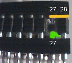 |
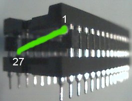
The connection drawn in green is the A14-addressline; on a Xicor X28C256P-20 E2PROM which i'm using, the pin 27 is used as the write-enable signal /WE, so we have to connect this pin to Vcc (+5V) (yellow connection).